
Designing the perfect printed circuit board (PCB) is not easy but a good PCB is essential to the work of an engineer. A good PCB has a high signal conductivity and a rationality of distribution and component selection.it is therefore a great necessity to have a great knowledge of the best techniques for routing and attaining high-speed signal circuits.
There are different high-speed design techniques engineers route the PCB design to acquire better productivity.
Using Multi-layer Boards
When engineers encounter decreasing circuit interference, they use a multilayer board to curb the problem. Multi-layer pcb circuit boards are made up of more than two superimposed copper electrical layers on top of each other and bonded together by resin layers. They are very complex but the best to use when increasing the package density of circuits that are integrated.
Many of the circuit layouts produce very unpredictable problems when designing. These problems are noise, cross talks, and stray capacities and so on. Engineers must therefore make PCB designs that minimise signal lines lengths and at the same time avoid parallel routing. A single sided or a double-sided PCB would not satisfactorily correct these mistakes. This is because a one sided or a double sided PCB has very limited crossover. To attain the best results and good performance, it is necessary to extend the PCB beyond this approach of two planes, hence the use of multi-layer PCB.
Shortening the Lead Pin between Components
PCB Basics
Making the lead in between components as short as possible reduces both distributed capacitor and inductance. In the process of routing, all through holes that are in the component connection should be as few as possible to increase circuit circulation.
Good PCB Schematic Creation
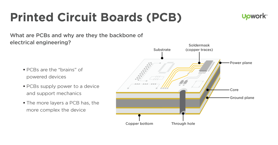
The Basics of Printed Circuit Board (PCB) Design
Laying out a good schematic whether you are designing the PCB layout yourself or outsourcing for a designer is another high-speed design technique to improve the circulation of the PCB.
Create a good schematic creation with an organised circuit flow that will be very critical in contributing to the high-speed design of a PCB.
The schematic with all parts and nets grouped correctly give a clear signal path for a circulatory flow of high-speed design.
A high-speed design schematic is in three parts, shown, as nets that are not similar which make up two circuits that are different. These two circuits are one signal. A good schematic should depict this very correctly when laying it on the PCB.
Protecting the Ground surrounding Signal Wires
Green Tech Innovations: Sustainable Living at its best
It is important to protect the ground surrounding all the signal wires when laying out a PCB routing design. There is a lot of interference from clock signals and analogue high-speed signals when routing. Add ground wire to protect routing from all these peripherals to enhance speed and clarity.
Take great caution when connecting a digital wire to a public ground wire because of the high frequency choke, which affects the speed of the PCB.
Engineers designing the PCB layout should avoid wiring of high-speed signal from forming stubs. High frequency should be carefully set between grounds, power wires so that in case there is any electromagnetic radiation, the radiation, the power and the bottom layers of the wires, absorbs and reduces it.
The above are some of the high-speed techniques to use in order to increase good and fast signal distribution when laying out the PCB layout design.